
 Rationale:
Rationale: 
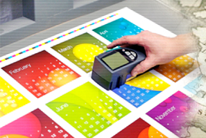
                This course provides an understanding of the basics related 
                to colour scanners, colour imaging systems, digital camera, computer-to-plate, 
                computer-to-print and digital proofing. Greater emphasis is laid 
                to understanding the reproduction process utilizing scanners, 
                operating systems, digital cameras & digital proofing.
                
                
Section I : Electronic Imaging


                  | Lesson 
                      No 1: IntroductionTheory.
 
 | Marks | Hours | 
                 
                  | 1.1 |  
                      Electronics and its importance | 2 | 1 | 
                 
                  | Lesson 
                      No 2: Structure of elementsTheory.
 
 | Marks | Hours | 
                 
                  | 2.1 |  
                      Electron | 3 | 2 | 
                 
                  | 2.2 |  
                      Energy of an electron
 | -- | -- | 
                 
                  | 2.3 |  
                      Valence electron | -- | -- | 
                 
                  | 2.4 |  
                      Free electron | -- | -- | 
                 
                  | 2.5 |  
                      Constant voltage source | -- | -- | 
                 
                  | 2.6 |  
                      Constant current source | -- | -- | 
                 
                  | 2.7 |  
                      Maximum power transfer Theorem  | -- | -- | 
                 
                  | Lesson 
                      No 3: Semiconductor physicsTheory.
 
 | Marks | Hours | 
                 
                  | 3.1 |  
                      Semiconductor | 9 | 8 | 
                 
                  | 3.2 |  
                      Bonds in semiconductor | -- | -- | 
                 
                  | 3.3 |  
                      Commonly used semiconductor | -- | -- | 
                 
                  | 3.4 |  
                      Types of semiconductor- Intrinsic and extrinsic – 
                        P and N type | -- | -- | 
                 
                  | 3.5 |  
                      PN Junction | -- | -- | 
                 
                  | 3.6 |  
                      Properties of PN junction | -- | -- | 
                 
                  | 3.7 |  
                      Applying voltage across PN junctioni) Forward biasing
 ii) Reverse biasing
 iii) Volt-amp characteristics
 
 | -- | -- | 
                 
                  | 3.8 |  
                      Terms- Breakdown voltage, Knee voltage | -- | -- | 
                 
                  | 3.9 |  
                      Limitations in the operating of PN junction | -- | -- | 
                 
                  | Lesson 
                      No 4: Semiconductor diodeTheory.
 
 | Marks | Hours | 
                 
                  | 4.1 |  
                      Crystal diode as rectifier
 | 4 | 4 | 
                 
                  | 4.2 |  
                      Resistance of crystal diode | -- | -- | 
                 
                  | 4.3 |  
                      Equivalent circuit of crystal diode | -- | -- | 
                 
                  | 4.4 |  
                      Crystal diode rectifier- Half wave and Full wave | -- | -- | 
                 
                  | 4.5 |  
                      Filter and types of filteri) Capacitor ii) Choke input iii) Capacitor input.
 
 | 3 | 2 | 
                 
                  | 4.6 |  
                      Zener diode, Zener diode as voltage stabilizer | 3 | 2 | 
                 
                  | Lesson 
                      No 5: TransistorTheory.
 
 | Marks | Hours | 
                 
                  | 5.1 |  
                      Naming the transistor terminals | 7 | 6 | 
                 
                  | 5.2 |  
                      Transistor action- working of npn and pnp transistor | -- | -- | 
                 
                  | 5.3 |  
                      Symbols | -- | -- | 
                 
                  | 5.4 |  
                      Common base connection-Characteristic of common base 
                        connection – input and output characteristics | -- | -- | 
                 
                  | 5.5 |  
                      Common emitter connection- input and output characteristics 
                       | -- | -- | 
                 
                  | 5.6 |  
                      Common collector connection | -- | -- | 
                 
                  | 5.7 |  
                      Comparison of Transistor connection | -- | -- | 
                 
                  | Lesson 
                      No 6: Modulation and DemodulationTheory.
 
 | Marks | Hours | 
                 
                  | 6.1 |  
                      Types of modulation and modulation factor | 2 | 2 | 
                 
                  | Lesson 
                      No 7: FET,SCRTheory.
 
 | Marks | Hours | 
                 
                  | 7.1 |  
                      Field effect transistor construction , Working of Junction 
                        field effect transistor , its advantages | 4 | 3 | 
                 
                  | 7.2 |  
                       Silicon controlled rectifier- working and application | 3 | 2 | 
                 
                  | 
  Reference 
                      Books 
 
  Electronics 
                      : V.K.Mehta 
  Section 
                      II : Digital Printing 
 
 
 | 
                 
                  | Lesson 
                      No. 1: Carrier Materials for ImagingTheory.
 
 | Marks | Hours | 
                 
                  | 1.1 |  
                      Electronics and its importance | -- | -- | 
                 
                  | 1.2 |  
                      Current carrier powders, their properties | -- | -- | 
                 
                  | Lesson 
                      No 2: Liquid Toner TechnologyTheory.
 
 | -- | -- | 
                 
                  | 2.1 |  
                      Introduction to different materials | -- | -- | 
                 
                  | 2.2 |  
                      Critical properties | -- | -- | 
                 
                  | 2.3 |  
                      Liquid Electrostatic toner charging | -- | -- | 
                 
                  | Lesson 
                      No 3: Dielectric papers and FilmsTheory.
 
 | Marks | Hours | 
                 
                  | 3.1 |  
                      Introduction to Electrography | -- | -- | 
                 
                  | 3.2 |  
                      Properties of Dielectric papers | -- | -- | 
                 
                  | 3.3 |  
                      Dielectric films | -- | -- | 
                 
                  | Lesson 
                      No 4: Photoreceptors – Selenium AlloysTheory.
 
 | Marks | Hours | 
                 
                  | 4.1 |  
                      Properties of Selenium and its alloys as Imaging Materials | -- | -- | 
                 
                  | 4.2 |  
                      Photoreceptor Design | -- | -- | 
                 
                  | Lesson 
                      No 5: Photoreceptors – Organic PhotoconductorsTheory.
 
 | Marks | Hours | 
                 
                  | 5.1 |  
                      Basic requirements for Xerography | -- | -- | 
                 
                  | 5.2 |  
                      Xerographic photoreceptors | -- | -- | 
                 
                  | 5.3 |  
                      Properties of Plasma-Deposited | -- | -- | 
                 
                  | 5.4 |  
                      Amorphous Silicon and its applications in electronic 
                        imaging | -- | -- |